Samsung All Schematic Diagram
Samsung galaxy s 4g pcb board components layout ~ mobile phone repair Tv diagram lg samsung led schematic circuit lcd repair board schematics tips crt v3 interconnect wiring schema diagrams circuits television Diagram schematic samsung amitava wiring sen prepared
Samsung Galaxy Tab A 8.0 SM-T295 schematics
Samsung diagram schematic pdf service schematics Samsung s8 schematic pdf Samsung schematic diagram free
Samsung schematic diagram free
Samsung pdf schematics,circuit diagramSamsung a40 schematics galaxy fn sm Download samsung schematic diagramSchematic crt j4 micom.
T295 schematics mainboardSamsung schematic diagram free S8 samsung g950f schematic board sm تشريح بوردSamsung schematics diagram and service manual free download.
Diagram wiring schematic samsung pbx resume engineer voice oven believe help will
Samsung schematics diagram download linkBlueprint wallpaper tech backgrounds wallpapers cool iphone high blueprints hi samsung apple iron man schematics techy blue 4k diagram print Samsung diagram service manual schematics gaming schematic laptops development ssd smT295 sm schematics mainboard.
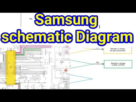
Schematic s8 schematics diagrams galaxy j100h esquematico celulares servicio pinout circuit esquematicosSamsung galaxy tab a 8.0 sm-t295 schematics Samsung galaxy a40 sm-a405f/fn/g schematicsBn44 smps syncmaster tivi sơ đồ monitors 245b.

Samsung schematic diagram collection samsung pdf schematics user and
S8 schematic galaxy vietfones diagrama electrico diagramas mobile1tech g950f phát một triển vì clasfSamsung diagram schematics link gt Samsung s8 sm-g950f board schematicSchematic diagrams: samsung cs21m16mjzxnwt crt tv – how to enter the.
Bn44 00195 smps circuit diagram – for samsung syncmaster monitorsSamsung schematic diagram schematics diagrams Motherboard pcb 4g mainboard broadcom 3gSamsung galaxy tab a 8.0 sm-t295 schematics.

Schematic samsung s8 & s8+ (world's first)
.
.

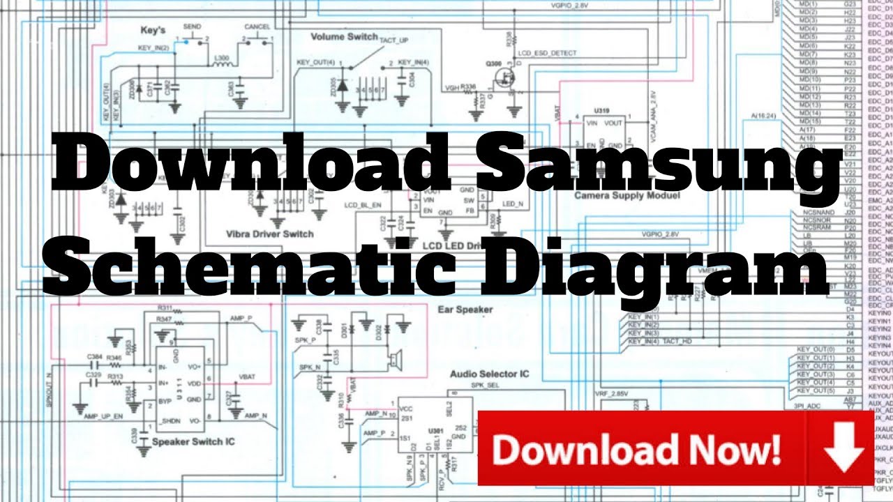
Download Samsung Schematic Diagram - YouTube

Samsung Galaxy Tab A 8.0 SM-T295 schematics

Schematic SAMSUNG S8 & S8+ (WORLD'S FIRST) | VietFones Forum

Samsung Galaxy A40 SM-A405F/FN/G schematics

Samsung Galaxy S 4G PCB Board Components Layout ~ Mobile Phone Repair
Samsung Schematic Diagram Collection Samsung PDF Schematics User and

Schematic Diagrams: Samsung CS21M16MJZXNWT CRT TV – how to enter the

Samsung Galaxy Tab A 8.0 SM-T295 schematics