Nand Gate Layout Cadence
Simulation of basic nand gate using cadence virtuoso tool Nand layout cadence virtuoso gate using tool Nand gate
Lab
How to draw 2 input nand gate layout in microwind Layout cadence nor cmos gate tutorial Nand gate study
Nand decoder gate multisim using
2-to-4 decoder using nand gateCmos 2 input nand gate Nand layout gate inputs result lvs labE77 . lab 3 : laying out simple circuits.
Gate nand logic function tables worksheet circuitNand gate circuits 1: a 2-input nand gate layout designed in cadence virtuoso.Layout geometries of 7nm finfet nand gates with l g =7nm and 9nm.
Layout nand gate cmos input glade
Hierarchical virtuoso lab5Cadence tutorial Virtuoso tutorial cadence layout inverter nand gate cmos pdf basicInfinitely expandable computing using three dimensional configurable.
Nand gate circuit and simulation in cadenceLayout nand gate cmos cadence lab simulation xor 421l ee tutorial through adder generated schematic going while below were Layout of nand gate using cadence virtuoso toolEe4321-vlsi circuits : cadence' virtuoso layout information.

Nand signals logic gates
Nand gate logic circuit truth table output expressed circuitglobeNand cadence virtuoso Ece429 lab5Cadence nand virtuoso gate simulation using.
Cmos nand complementaryGlade tutorial Nand cmos gate input layout microwind pspiceLab 6 ee 421l spring 2015.

Multisim nand
What is nand gate?2: complementary cmos three-input nand gate. Cadence virtuoso vlsiCadence schematic gate layout cmos nand assura verification.
Nand cadence virtuoso gate lvs layout stack problems vlsi schematic integrated circuitNand finfet 7nm 9nm geometries respectively 1: a 2-input nand gate layout designed in cadence virtuoso.Nand gates nor logic using gate dimensional three preference computing infinitely configurable expandable into turn other built plus.

Cadence tutorial
Layout nor cadence gate lab6Cadence tutorial -cmos nand gate schematic, layout design and physical Combinational circuits & functions: construction & conversionNand gate layout microwind input draw lw.
Integrated circuitPicture and function of nand gate digital logic Nand gate cadenceNand layout gate simple laying circuits larger figure version click.


Simulation of Basic NAND Gate using Cadence Virtuoso Tool - YouTube

Cadence tutorial - Layout of CMOS NOR gate - YouTube

How to draw 2 input NAND gate layout in Microwind - YouTube

1: A 2-input NAND gate layout designed in Cadence Virtuoso. | Download

Cadence tutorial - Layout of CMOS NAND gate - YouTube

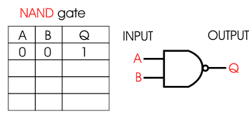
What is NAND Gate? - Logic Circuit & Truth Table - Circuit Globe

CMOS 2 input NAND gate | All For Students