How To Convert Schematic To Pcb Layout In Altium
Altium pcb layout Altium pcb pcbs thousand Pcb design software: which one is best?
How to Create a PCB Layout from a Schematic in Altium Designer | PCB
Tutorial schematic altium pcb designer embedded engineering system continue layout next make will How to create a pcb schematic How to create a pcb layout from a schematic in altium designer
Altium designer pcb tutorial example component embedded engineering system position move location place them right
Schematics according restore raypcb convert protel orcadEmbedded system engineering: altium designer tutorial 3 Learning pcb design in one weekLearn altium essentials.
Altium schematic convertAltium pcb learning week schematic monitors both complete left board Embedded system engineering: altium designer tutorial 4How to create a pcb layout from a schematic in altium designer.
Pcb cad software component board electrical layout reverse engineering which module diptrace symbol
How to create a pcb layout from a schematic in altium designerAltium pcb schematic Altium schematic pcb designer capture tutorial layoutEasyeda software convert presented.
Getting started with easyeda part 3: pcb layoutDesign pcb layout and schematic using altium,pads,easyeda by vipreteam Altium transferred beenAltium pcb schematic layout using pads easyeda will screen.

Altium designer tutorial: schematic capture and pcb layout (1of2)
How to convert pcb to schematic diagram? .
.


Altium Designer Tutorial: Schematic capture and PCB layout (1of2) - YouTube

Getting Started with EasyEDA Part 3: PCB Layout - Shawn Hymel

Learning PCB design in one week - We have the Technology
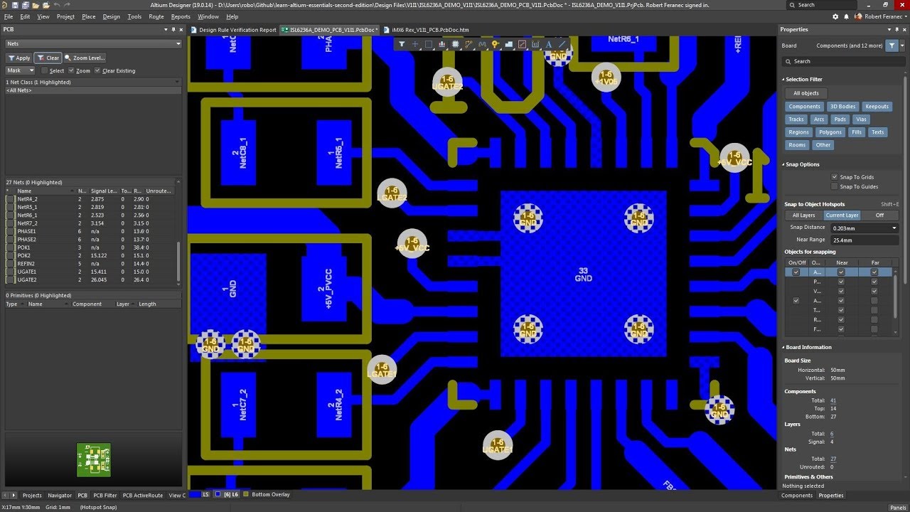
Learn Altium Essentials - Doing PCB Layout (Lesson 4) - Second Edition

How to Create a PCB Layout from a Schematic in Altium Designer | PCB

How to Create a PCB Layout from a Schematic in Altium Designer | PCB

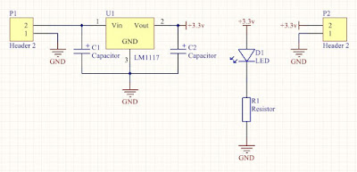
How to Create a PCB Schematic | Altium Designer

PCB Design Software: Which One is Best?

How to Convert PCB to Schematic Diagram? - RAYPCB